
|
Home |
|
History |
|
Techniques |
|
Applications |
|
community |
|
Projects |
|
Publications |
|
Conferences |
|
Softwares |
|
Contact Us |
|
History |
|
|

|
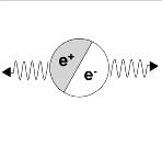
The positron as the antiparticle of the electron was predicted by Dirac ("On the quantum theory of electron":1928). First experimental indications of an unknown particle were found in cloud-chamber photographs of cosmic rays (Anderson 1932). This particle was identified later as the positron, which was thus the first antiparticle in physics. The annihilation of the positron with electrons in matter was first studied in the 1940s. It was discovered early that the energy and momentum conservation during the annihilation process could be utilized to study properties of solids. The bound state of a positron and an electron, as the lightest known atom to be formed, is analogous to a hydrogen atom, where the proton is replaced by the positron. This e+-e- state is called positronium (Ps). It was predicted by Mohorovicic (1934) and discovered by Deutsch (1951).
The early experiments with positrons were dedicated to the study of the electronic structure, e.g. the Fermi surface in metals and alloys (Behringer and Montgomery 1942; de Benedetti et al. 1950). The various experimental techniques of positron annihilation based upon the equipment of nuclear spectroscopy were developed strongly in the two decades after 1945. In addition to the angular correlation of annihilation J-quanta, Doppler broadening of the annihilation line and positron lifetime spectroscopy were established as independent methods. It was realized by the end of the 1960s that the annihilation parameters are sensitive to lattice imperfections. It was discovered that the positron may be trapped in crystal defects, i.e. the wave function of the positron is localized at the defect site until annihilation. This behavior of positrons was clearly demonstrated by several authors, e.g. MacKenzie et al. (1967) for thermal vacancies in metals, Brandt et al. (1968) in ionic crystals, and Dekhtyar et al. (1969) after plastic deformation of semiconductors. The investigation of crystal defects has become the dominant issue of positron annihilation studies. This development is illustrated in the Figure, which shows the number of published papers on defect studies with positrons. The number of papers has increased continuously. Up to the mid-1980s, defect studies in solids were mainly carried out in metals and alloys. The experience obtained in this field was applied to semiconductors. The study of defects in compound and elemental semiconductors amounts now to about the half of the total number of papers on defect studies with positrons.
The trapping of the positron in defects is based on the formation of an attractive potential at open-volume defects, such as vacancies, vacancy agglomerates, and dislocations. The main reason for this potential is the lack of a repulsive positively charged nucleus in such a defect. The sensitivity range for the vacancy detection in metals starts at about one vacancy per 107 atoms. This enormous sensitivity is caused by the fact that the positron diffuses about 100 nm through the lattice and probes a high number of atoms until annihilation. When the positron is trapped in an open-volume defect, the annihilation parameters are changed in a characteristic way. The positron lifetime increases in an open-volume defect due to the lower electron density. Momentum conservation during gamma-annihilation leads to a small angular spread of the collinear J-quanta or a Doppler shift of the annihilation energy. Both properties, the density and the momentum distribution of electrons participating in the annihilation, result in observables to be detected in a positron experiment. The analysis of the annihilation radiation thus gives the possibility of defect detection. Clustering of vacancies as a typical defect reaction may be observed as the increase in the defect-related lifetime due to the further decrease in the electron density.
The positron trapping behavior in semiconductors is more complex compared with metals. This is mainly due to the fact that the positron as a charged particle is sensitive to the charge state of defects. The defect identification is more difficult in compound semiconductors since the variety of point defects increases. The simple transfer of the knowledge obtained in metals gave rise to some confusing results and misinterpretations at the beginning of semiconductor studies with positrons. The trapping coefficient as the sensitivity-scaling factor taken from metals gave vacancy concentrations that were too high. Since then, reliable experiments have been carried out to determine the trapping coefficient in semiconductors. The improvement of the theoretical understanding of positron trapping, due especially to M. Puska and R. Nieminen (for a review see Puska and Nieminen 1994), the refinement of positron lifetime spectroscopy as the main technique for defect studies, and the increasing amount of data have made it possible to give reliable qualitative and quantitative information on defects in semiconductors. A large number of investigations have been carried out for differently grown bulk semiconductor crystals. Irradiation with high-energy electrons at low temperature represents an important tool for defined generation of point defects. Many positron studies on the defect structure of semiconductors have been carried out after such irradiation. Practically all positron lifetimes for the important bulk semiconductor materials and many lifetimes for various vacancy-type defects have been experimentally determined. In comparison with theoretical calculations, the defects can be characterized by their specific positron lifetimes. A promising new development is the background-reduced measurement of positron annihilation with core electrons by Doppler-broadening coincidence spectroscopy. It seems to be possible to obtain chemical information on the surroundings of the annihilation site by comparison of measured and theoretically calculated Doppler spectra in the highmomentum region. The sublattice of the defect and eventually the type of impurities stabilizing the defect complexes may be determined. A newer development is the use of ratio or difference curves of the Doppler-broadened annihilation lines as fingerprints for specific annihilation sites. The charge state of vacancies in semiconductors strongly influences the sensitivity range of positron annihilation. Positively charged vacancies repel positrons and are thus invisible to the different positron-related defect detection methods. The sensitivity range for neutral vacancies in semiconductors is similar to that for metals. The attractive potential of the vacancy is superimposed on the Coulomb potential of negatively charged vacancies. This results in a higher sensitivity of positrons at low temperatures and in a pronounced temperature dependence of positron trapping.
In principle, dislocations are also positron traps in semiconductors. However, the sensitivity range is comparable to that of metals and, hence, dislocations can be observed only after plastic deformation. Precipitates were found to be positron traps in some alloys. Their density is normally too low to be detected in semiconductors. In addition to the positron traps known from metals, negatively charged nonopen- volume defects, e.g. acceptor-type impurities or negatively charged antisites in a compound, represent positron trapping centers at low temperatures. The Coulomb potential of these defects is responsible for the formation of shallow Rydberg states. Positrons may be bound with a small binding energy to such centers, which are called shallow positron traps. In summary, neutral and negative vacancy-type defects, as well as negative ions, are the dominant positron traps in semiconductors. Temperature-dependent lifetime measurements may distinguish between both defect types. However, it should be noted that the main advantage of positron annihilation is the sensitive detection of open-volume defects. This defines the power of the positron methods in contrast to most electrical and optical spectroscopies. On the other hand, it may also be a disadvantage, as important defect types, such as interstitials and neutral or positive impurities or antisites, remain in the dark. Modern semiconductor devices are based on layered structures, such as epitaxially grown layers, oxides, or implanted layers. The disadvantage of conventional positron techniques directly utilizing positrons from the betta-decay of a radioactive source is the broad energy distribution and the large penetration depth of positrons in the sample. Consequently, only bulk material can usually be investigated. This drawback has been overcome by the development of the slow-positron-beam technique. This is based on the moderation of positrons. Monoenergetic positrons are obtained at surfaces exhibiting a negative positron work function, e.g. tungsten. The emitted positrons are guided as a beam to the sample. The variation of the incident positron energy in an accelerator stage enables the measurement of nearsurface defect profiles. The positron beam can be pulsed and thus the positron lifetime can be measured too. The focusing of the positron beam may in future allow the three-dimensional probing of defect structures, i.e. the development of a positron microscope and microprobe. |